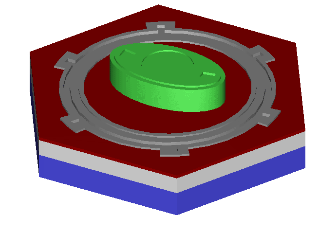
The semiconductor industry has refined precision over 50 years, from microns to nanometers. Much of this art is known as thin-film processing-- Deposit, pattern, etch, repeat. Today, this achieves nanometer dimensions and tight tolerances. Lateral (x,y) patterns are mask/lithography-defined, while depth (z) is usually defined by a deposition or etch step. This yields a "2.5 Dimensional" structure-- the third dimension is only controlled in discrete steps. This describes most Integrated Circuits today.

This same magnitude of precision is achieved using Ultra-Precision Machining, or Diamond Turning. Here, true freeform 3D is the norm, but parts are made one-by-one. Diamond turning can be used to produce molds, which can then replicate 3D parts in volume.
At Applications Laboratory, we merge our experience in these areas, as well as metrology expertise down to atomic scale, to realize novel 3D structures, often possesing quantum and unique optical properties. Applications Laboratory can design, fabricate and test precision Semiconductor, Optical, Quantum and MEMS devices.